|
 Pulse Voltage: -10V-+10V, Pulse Width: 0-200ms Pulse Voltage: -10V-+10V, Pulse Width: 0-200ms
Precise path and location
Customized BMP image
Maximum Load: 3×10⁵nN
Any desired complicated pattern on Nano-scale
|
|
| |
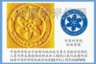
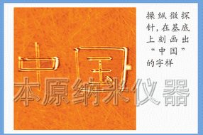
Graphical Nano-lithography |
| |
The software allows user to create any desired pattern simply by loading in a BMP graph with the electro-oxidation technique.
|
|
|
| |
Nano-Embrassing |
| |
The idea is to imprint a pattern on the surface using the prepared piece of nanostructured material (stamp) which is pressed against the surface leaving a characteristic pattern behind.
|
|
| |
|
| |
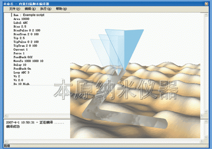
Vector Scan |
| |
The software provides a set of commands that permit users to control all signals such as voltages, currents, pressures and forces.
|
|
| |
|
| |
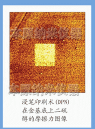
Dip-Pen Nano-lithography |
| |
A tip of the AFM can be used as a 'pen'. The tip is coated with thin film of molecules. During the process of tip movement, the molecules migrate from tip to surface and make a nanoscopic pattern on the surface.
|
|